

")


innovative optoelectronics,
nanotechnology and
ultimate vacuum
Scanning electron microscopy (SEM) is an observation method used as an important analytical technique in the physical, chemical and biological research. Compared with light microscope, SEM uses narrow focused high energy electron beam scanning across the surface of the sample to image objects at much greater magnification and resolution. SEM provides images with magnifications rate of 200 ~X1,000,000, which makes it a particularly important and powerful tool for visualizing sub micron-scale features. Electron beam excites atoms on the surface of the sample and thereby generates various physical information, which then is reimagined providing detailed high resolution images for the characterization of the material’s morphology.
The most common SEM detects secondary electrons (SE) and backscattered electrons (BSE) generated by beam. SE are emitted by atoms of the material through the interaction between the electron beam and the sample. BSE are the incident electrons that bounce out of the sample. They have a low energy and they are able to show differences in absorption between elements, therefore their detection helps to identify areas of differing nature in the sample.
When combined with other detecting techniques, such as energy-dispersive X-ray spectroscopy (EDX or EDS), SEM exhibits greater impact on sample analysis and visualization. EDS detector measures the energy of the emitted photons in the X-ray electromagnetic spectrum and provides accurate information about elemental identification and elemental quantitative composition on microscopic surface structures of the sample.
SEM imaging coupled with EDS data gives a possibility to form X-ray map of data to present areas of distribution of individual elemental concentrations.
Combination of these two techniques is suitable for almost all kinds of samples and has a wide range of applications from scientific research to quality control.
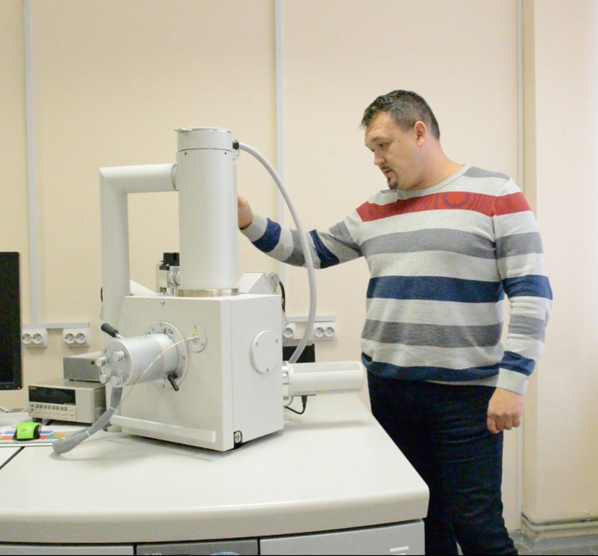
Manufacturer / type – scanning electron microscope QUANTA INSPECT, Thermo Fischer Scientific (FEI)
Resolution:
– 3 nm for acceleration voltage up to 30 KV (high vacuum, SE)
– 3 nm for acceleration voltage up to 30 KV (low vacuum, SE)
Magnification: 14 to 1000000 x
Acceleration voltage: 200 V to 30 kV
Detectors: Everhart-Thornley SE, in-lens SE, BSE-detector with high resolution, STEM
Energy-dispersive X-ray spectroscopy (EDX) by Oxford Instruments
5 axis stage and big sample chamber
“Low-Vacuum”- operation for analysis of low conducting specimens
Spelling error report
The following text will be sent to our editors: